Language:


In contrast to previous calculators, where mechanical or elctro-mechanical triggers were used, today's digital applications use electronic triggers based on semiconductors. In this chapter the physical fundamentals of semiconductors are explained in order to use them in the next chapter (→ MOSFET-Transistors).
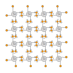 Semiconductors are materials that have both conducting and isolating properties. The most popular representative is the element silicon (Si). Every phenomenom will be explained with this element. Silicon is a quadrivalent element, i.e. is has four valence electrons. To achieve a noble gas configuration with eight valence electrons each Si-atom tries to bond with four other atoms where a pair of electrons is used by both atoms. The resulting structure is pretty stable - a crystal lattice comes to being. Every charge carrier ist bond. Because there are no moveable charge carriers, no current is able to flow, the semiconductor appears as a isolator.
However this structure comes to being only at temperatures near the absolute zero (≈ -273 °C). At higher temperatures some electrons may be able to switch to a higher energy level. When they have enough energy, they are able to break the bond and move freely as negative charge carriers. At their former place they leave a so called hole. Neighbouring electrons can jump in that hole leaving their former place where another hole is being created. The hole can flow virtually and appears as a positive charge carrier. Because now there are freely moveable charge carrier, a current can flow. The higher the temperature is, the better the semiconductor conducts.
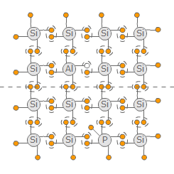 In order to influence the conductivity of semiconductors specifically it is possible to insert some foreign atoms into the crystal lattice. This proceduure is called doping. Using the quadrivalent silicon as the base material either trivalen or pentavalent atoms can be inserted.
Doping with trivalent elements like aluminium results in another hole in the crystal lattice. The aluminium atom also tries to achieve the nobel gas configuration but therefore lacks one electron. Only if another electron is inserted in the lattice from outside, the aluminium atom can achieve its nobel gas configuration. The additional hole appears as a additional positive charge carrier so the conductivity improves. Because an additional positive charge carrier is inserted this kind of doping is called p-doping
On the other hand, if a pentavelant atom like phosphor is inserted, there is one electron more than necessary. This electron appears as an addtional negative charge carrier and improves the coductivity of the semiconductor. Because a negative charge carrier is added this kind of doping is called n-Doping.
If n-doped and p-doped areas are put on one another, at the barrier it comes to recombination: The additional electrons from the n-area fill the holes in the p-area. Positive charged holes and negative charged electrones recombine und become part of the bond. This happens until there are no more moveable charge carriers along the barrier wich will result in an isolation area.