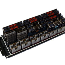
IBM designed custom hybrid circuits using flip-chip mounted, glass encapsulated transistors and diodes with silk screened resistors on a 0.5" ceramic substrate. The encapsulation in glass brought the advantage, that a hermetically sealed package wasn't necessary anymore to guaranty a long product life and a high reliability.The placement of the devices was accomplished by automatic placement machines, followed by a reflow-soldering-process, where the devices were connected with contact-fields on the circuit board. A ceramic module accommodated space up to 6 transistors with the associated resistors, capacitors and inductors. The produced circuits were either encapsulated in plastic or covered with a metal lid. Several of these hybrid circuits were then with other devices mounted on a small multi-layer printed circuit board to make an SLT module. There were modules with 6, 12 and 24 hybrid circuits on it. Each SLT module had a socket on one edge that was plugged into a SLT-Board. Those boards were available in several dimensions, depending on the amount of the circuits boards, that should plugged on it.
